The thick film refers to the thickness of conductor layer on ceramic pcb.
Thick film ceramic pcb.
Thick film hybrid circuits are made using a print fire p f technique.
Our precision etching technology pushes thick film ceramic substrates to a best in class position offering the tightest tolerances and the highest performances rivaling thin film capabilities.
Here are some steps about the fabrication of thick film ceramic pcb.
The conductor is silver or gold palladium and was printed on ceramic substrate.
Thin and thick film resistors are the most common types in the market.
This involves a combination of multi layer screen printing of precious and semi precious metals au ag pd as well as the firing of tracks and precision resistors onto a range of ceramic and metal substrates.
Therefore the thick film circuit has stronger external environment adaptability than independent soldering circuit.
They are characterized by a resistive layer on a ceramic base.
The metal deposition methods used in vacuum processes and the flexibility that can be achieved in terms of thickness and type of metallization in particular really set thin film technology apart from printed circuit board technology.
Although their appearance might be very similar their properties and manufacturing process are very different.
If it s possible in thin film chances are it can be realized in etched thick film at a fraction of the price.
Thick film gold paste and dielectric paste is repeatedly and alternately printed on ceramic base and goes through baking at a temperature below 1000 c.
What are thick film circuit boards.
Ceramic material pcb available open cooling application the development of the industry because of the ceramic substrate cooling characteristics combined with ceramic substrates with high heat dissipation low thermal resistance long service life the advantages of resistance to voltage with the improved production technology equipment product prices accelerate rationalization and.
Thin film technology uses semiconductor and microsystem technology processes to produce circuit boards on ceramic or organic materials.
Thick film ceramic pcb.
A thick film ceramic board.
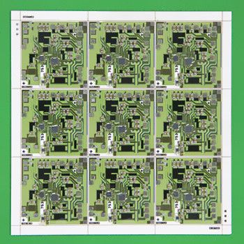
The size of the common ceramic substrate is 114 114mm.
Typically thick film circuit substrates are al 2 o 3 alumina beryllium oxide beo aluminum nitride aln stainless steel sometimes even some polymers and in rare cases even silicon si coated with silicon dioxide sio 2 most used substrates for a thick film process are either 94 or 96.
A typical thick film process would consist of the following stages.
More for thick film ceramic pcb.
Since the thick film ceramic pcb possesses many benefits then how to make it.
Although this type of fabrication technology is optimal to large scale ceramic pcb manufacturing and features relatively high assembly base number its application is limited due to high cost.
The naming originates from the different layer thicknesses.
What are thin and thick film resistors.